text to clipboard
Nanomaterial growth platform's end-to-end processing purity offers breakthrough for developers targetting commercial manufacturing
incorporates nine of the top processes used in nanomaterial development
first platform to maintain vacuum from catalyst delivery to material growth
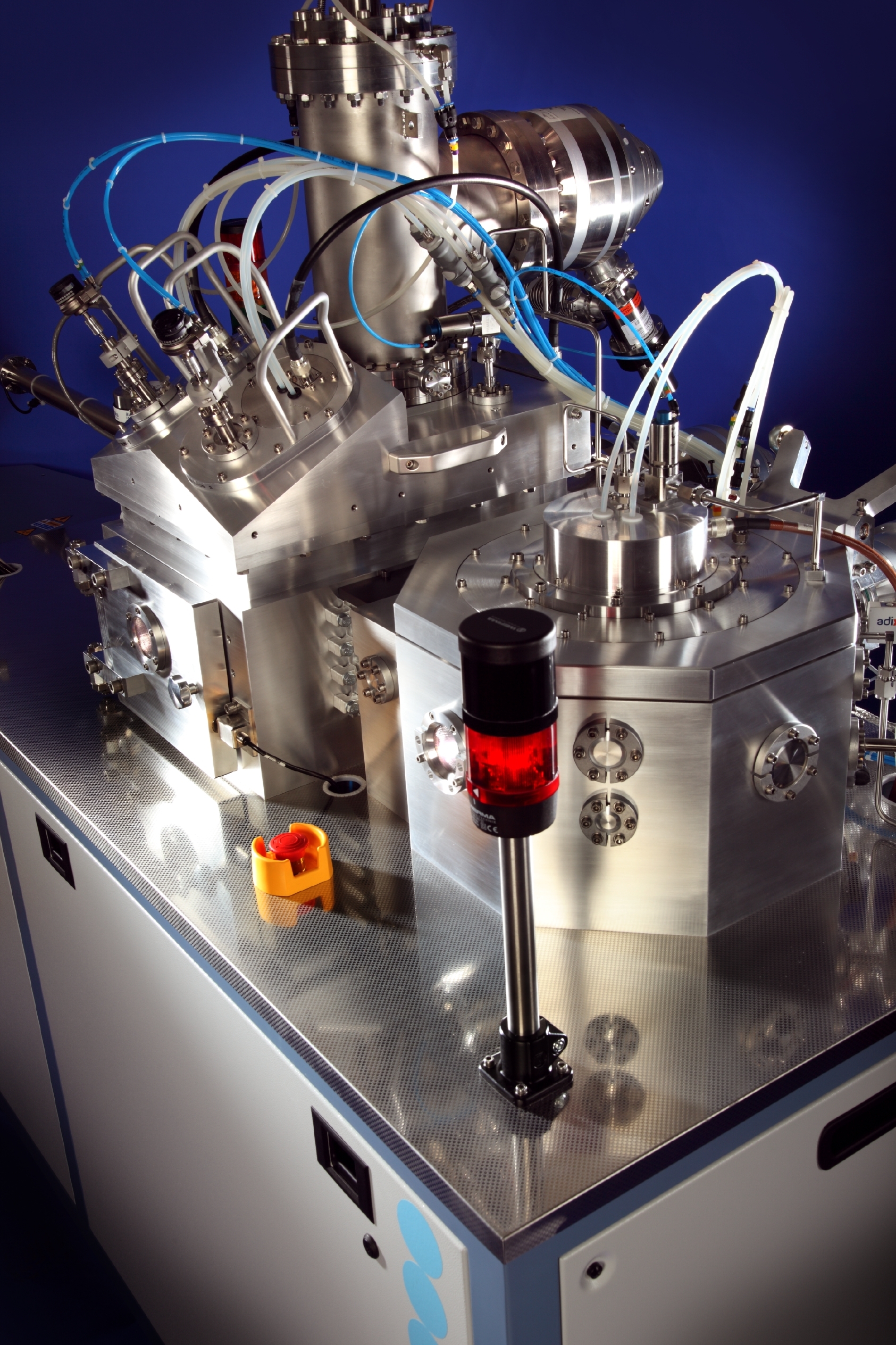
Newhaven, UK, July 6, 2010 --- Today, Surrey NanoSystems sets a new benchmark for the production of nanomaterials with the launch of an automated and exceptionally versatile growth platform, NanoGrowth-Catalyst. Incorporating nine advanced nanomaterial processing techniques, the platform can synthesise an exceptional variety of nanomaterials including graphene, nanowires and carbon nanotubes.
Application versatility is enhanced by a multi-chamber design - a first in this industry sector - that ensures the purest processing conditions by continuously maintaining the substrate under vacuum from deposition of catalysts to growth of nanomaterials. This end-to-end vacuum processing is critical for the precursors and catalysts used for nanomaterials, which are easily contaminated by exposure to atmosphere.
"Surrey NanoSystems entered the business world with a groundbreaking platform combining both CVD and plasma-enhanced CVD nanomaterial growth techniques," says Ben Jensen of Surrey NanoSystems. "This new platform takes processing flexibility much farther. It offers the means to support and speed research across the spectrum of nanomaterials, combined with automated handling and control to help developers turn material growth ideas into practical and repeatable production processes."
NanoGrowth-Catalyst will replace multiple pieces of equipment with a single automated system. The processing techniques supported by the new platform are: LPCVD (low-pressure chemical vapour deposition) and PECVD (plasma-enhanced CVD), sputtering, sputter etching and ashing, delivery of solid- or liquid-phase catalysts/precursors, creation of controlled-density nanoparticle catalysts at room temperature, thermal annealing, rapid thermal processing (RTP), and a unique form of rapid thermal growth for nanomaterials called RTG which has been developed to prevent agglomeration of catalyst particles.
The platform also supports broadband substrate degassing to remove surface contaminants before processing - helping to ensure the optimum adhesion of catalysts and films. An inductively coupled plasma source can additionally be fitted as an option - at the time of purchase or during the platform's lifecycle - to optimise the generation of sensitive materials employed in growth processes.
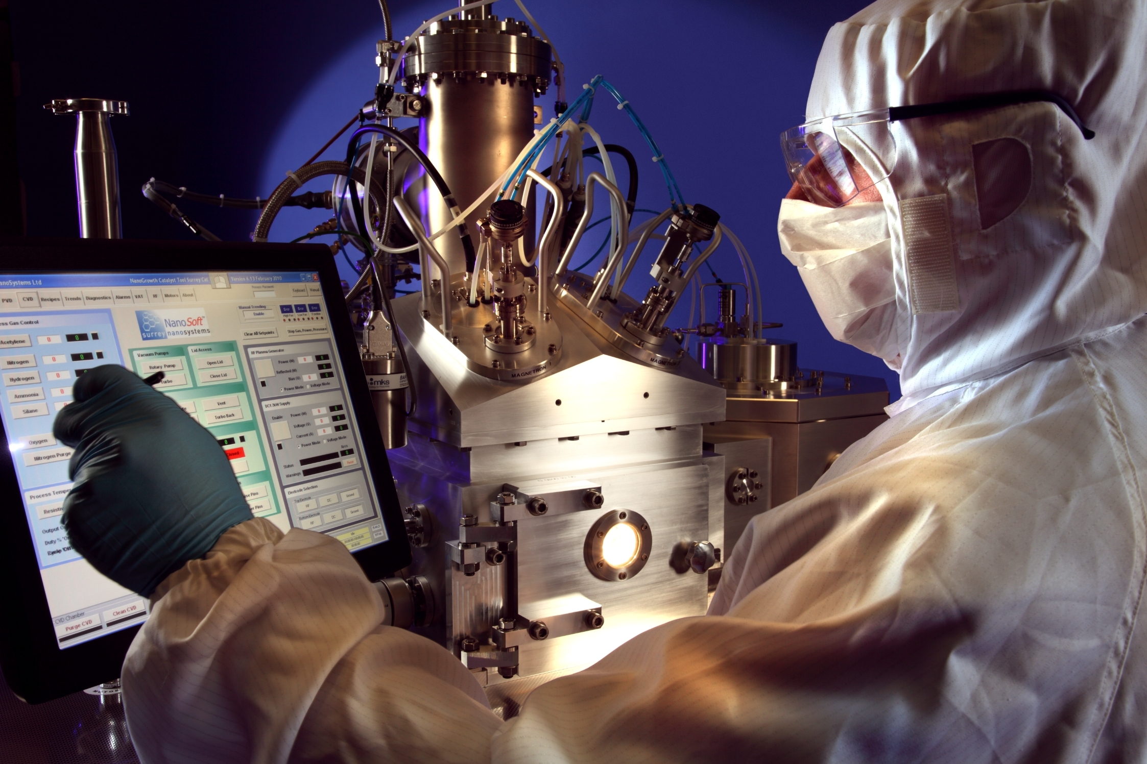
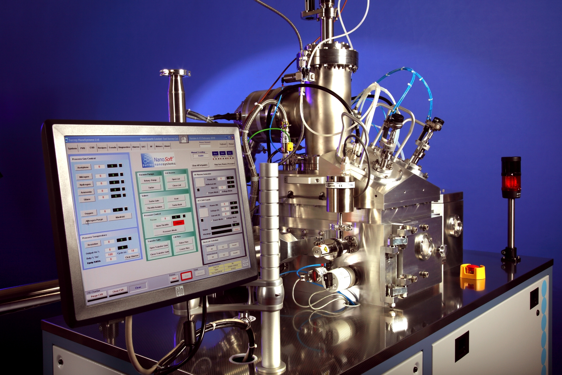
A highly graphical interface gives users complete control over the processing parameters and steps. With its range of techniques users can employ NanoGrowth-Catalyst for creating or delivering growth catalysts and precursors (the sputtering platform's dual magnetrons also support co-deposition), depositing nanoparticles at room temperature, catalyst or material activation, growing materials, etching, and deposition of active or passive barrier films.
The system has three chambers: a load/lock chamber and two reaction chambers, plus an automatic transport system for moving wafers/substrates. End-to-end atmosphere-free processing ensures the highest purity conditions to minimise contamination and oxidation and ensure consistent and repeatable results. Despite its extensive capability, NanoGrowth-Catalyst occupies only a very small cleanroom footprint of 1 x 2 m.
The specification for this richly equipped platform came partly from requests by users of Surrey NanoSystems' first growth platform, the single reaction chamber NanoGrowth 1000n, and from researchers at Surrey NanoSystems and its research partner, the Advanced Technology Institute at the University of Surrey.
In addition to making growth platforms, Surrey NanoSystems is engaged in developing nanoelectronics materials and processes to support the continued scaling of semiconductor devices. NanoGrowth-Catalyst's automated handling and wealth of processing capabilities are seen as the ultimate platform to support the company's own research into nanomaterial growth at temperatures compatible with mainstream CMOS fabrication. The company has already made significant advances in developing practical techniques for fabricating interconnection vias and low-k dielectrics for inter-layer insulation - key challenges on the semiconductor industry's roadmap as process geometries shrink.
"We expect this new growth tool to shorten the time to market for researching nanomaterials and applying them to commercial products," adds Ben Jensen. "There is nothing to compare with it on the market today and it offers a uniquely powerful means of investigating and developing nanomaterial technologies."
Surrey NanoSystems has already received advance orders for the new NanoGrowth-Catalyst, and is currently manufacturing an initial batch of three systems.
http://www.surreynanosystems.com
Media contact:
Ben Jensen, CTO, Surrey NanoSystems
t: +44 (0) 1273 515899
e: b.jensen@surreynanosystems.com
Surrey NanoSystems, Euro Business Park, Building 24, Newhaven, BN9 0DQ, UK. t: +44 (0)1273 515899; enquiries@surreynanosystems.com; http://www.surreynanosystems.com
NanoGrowth is a registered trade mark of Surrey NanoSystems.


 |
|